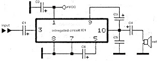
Showing posts with label amplifier. Show all posts

Monday, September 2, 2013

1W Audio Amplifier Using NCP2830

This 1w audio amplifier circuit is designed using NCP2830 audio IC manufactured by ON Semiconductor.This audio power amplifier ic designed for portable communication device applications and require few external electronic components.

1W Audio Amplifier Circuit using NCP2830 


NCP2830 is capable to provide 1W continuous output power in 8 ohms load.NCP2830 audio power amplifier main features are : high quality audio (THD+N = 0.04%) , low noise: SNR up to 100 dB, overall system efficiency optimization: up to 89% , Superior PSRR (−88 dB): Direct Connection to Battery , Very Low Quiescent Current 7 mA , Optimized PWM Output Stage: Filterless Capability , Selectable gain of 2 V/V or 4 V/V .
Continue reading...

Monday, May 13, 2013

Battery powered Headphone Amplifier

Some lovers of High Fidelity headphone listening prefer the use of battery powered headphone amplifiers, not only for portable units but also for home "table" applications.

Battery-powered Headphone Amplifier
Parts:

P1_____________22K Dual gang Log Potentiometer (ready for Stereo)

R1_____________15K 1/4W Resistor
R2____________100K 1/4W Resistor
R3____________100K 1/2W Trimmer Cermet
R4_____________47K 1/4W Resistor
R5____________470R 1/4W Resistor
R6____________500R 1/2W Trimmer Cermet
R7______________1K 1/4W Resistor
R8,R9__________18K 1/4W Resistors
R10,R11_________2R2 1/4W Resistors
R12____________33R 1/4W Resistor
R13_____________4K7 1/4W Resistor

C1,C2__________10µF 25V Electrolytic Capacitors
C3,C5_________100nF 63V Polyester Capacitors
C4,C6_________220µF 25V Electrolytic Capacitors

Q1,Q2,Q5______BC560C 45V 100mA Low noise High gain PNP Transistors
Q3,Q4_________BC550C 45V 100mA Low noise High gain NPN Transistor
Q6____________BC327 45V 800mA PNP Transistor
Q7____________BC337 45V 800mA NPN Transistor

SW1____________SPST slide or toggle Switch

J1_____________RCA audio input socket
J2_____________6mm. or 3mm. Stereo Jack socket

B1_____________6V Battery (4xAA or AAA Alkaline or rechargeable cells, etc.)


Output power can reach 100mW RMS into a 16 Ohm load at 6V supply with low standing and mean current consumption, allowing long battery duration.
The single voltage gain stage allows the easy implementation of a shunt-feedback circuitry giving excellent frequency stability.


Notes:

* For a Stereo version of this circuit, all parts must be doubled except P1, SW1, J2 and B1.
* Before setting quiescent current rotate the volume control P1 to the minimum, Trimmer R6 to maximum resistance and Trimmer R3 to about the middle of its travel.
* Connect a suitable headphone set or, better, a 33 Ohm 1/2W resistor to the amplifier output.
* Switch on the supply and measure the battery voltage with a Multimeter set to about 10Vdc fsd.
* Connect the Multimeter across the positive end of C4 and the negative ground.
* Rotate R3 in order to read on the Multimeter display exactly half of the battery voltage previously measured.
* Switch off the supply, disconnect the Multimeter and reconnect it, set to measure about 10mA fsd, in series to the positive supply of the amplifier.
* Switch on the supply and rotate R6 slowly until a reading of about 3mA is displayed.
* Check again the voltage at the positive end of C4 and readjust R3 if necessary.
* Wait about 15 minutes, watch if the current is varying and readjust if necessary.
* Those lucky enough to reach an oscilloscope and a 1KHz sine wave generator, can drive the amplifier to the maximum output power and adjust R3 in order to obtain a symmetrical clipping of the sine wave displayed.


Technical data:

Output power (1KHz sinewave):
16 Ohm: 100mW RMS
32 Ohm: 60mW RMS
64 Ohm: 35mW RMS
100 Ohm: 22.5mW RMS
300 Ohm: 8.5mW RMS
Sensitivity:
160mV input for 1V RMS output into 32 Ohm load (31mW)
200mV input for 1.27V RMS output into 32 Ohm load (50mW)
Frequency response @ 1V RMS:
flat from 45Hz to 20KHz, -1dB @ 35Hz, -2dB @ 24Hz
Total harmonic distortion into 16 Ohm load @ 1KHz:
1V RMS (62mW) 0.015% 1.27V RMS (onset of clipping, 100mW) 0.04%
Total harmonic distortion into 16 Ohm load @ 10KHz:
1V RMS (62mW) 0.05% 1.27V RMS (onset of clipping, 100mW) 0.1%
Unconditionally stable on capacitive loads
Continue reading...

Thursday, April 11, 2013

5 8 Watt audio power amplifier

5,8watt amplifier schematics
This amplifier circuit has a power output of a small or too low at 5.8 Watt, which uses IC KA2205. The required voltage for at least 6 volts to 18 volts DC maximum.


Schematics power audio amplifier with IC KA2205

low power amplifier
Component List
C1 = 1uF
C2 = 100uF
C3 = 47uF
C4 = 1000uF
C5 = 0.1uF
C6 = 220uF
IC1 = KA2205

Continue reading...

Tuesday, April 9, 2013

TDA2822 made for 5 1 audio amplifier system

Skema Rangkaian Circuit combination of the 3 IC TDA2822  above can be used for 5.1 audio power amplifier system with low power output . The input signal used is analog signal not digital (SPDIF) , so it needed some input to the jack input. The speakers are suitable for use have impedance 8 Ohms , and with power 4 Watt, to Left , Right , Rear pair , center , and subwoofer speakers. To run this circuit , is also required circuit for volume control as tone control.


Component and technical Information :
C1-C6 : 220uF/25V
C7-C9 : 47uF/16 V
IC       : TDA2822 x3
CON-1: VCC +12volts DC
CON-2: Ground
CON-3: Left Speaker
CON-4: Right Speaker
CON-5: Rear Speaker
CON-6: Rear Speaker
CON-7: Center Speaker
CON-8: Subwoofer Speaker
X1-1:Ground
X1-2:Subwoofer Input
X1-3:Center Input
X1-4:Rear Input
X1-5:Rear Input
X1-6:Right Input
X1-7:Left Input

See this Printed circuit board below:

circuit and PCB Design use Cadsoft Eagle Software
Continue reading...

Sunday, March 24, 2013

Hybrid Headphone Amplifier


Potentially, headphone listening can be technically superior since room reflections are eliminated and the intimate contact between transducer and ear mean that only tiny amounts of power are required. The small power requirement means that transducers can be operated at a small fraction of their full excursion capabilities thus reducing THD and other non-linear distortions. This design of a dedicated headphones amplifier is potentially controversial in that it has unity voltage gain and employs valves and transistors in the same design.

Normal headphones have an impedance of 32R per channel. The usual standard line output of 775 mV to which all quality equipment aspires will generate a power of U2 / R = 0.7752 / 32 = 18 mW per channel across a headphone of this impedance. An examination of available headphones at well known high street emporiums revealed that the sensitivity varied from 96 dB to 103db/mW! So, in practice the circuit will only require unity gain to reach deafening levels. As a unity gain design is required it is quite possible to employ a low distortion output stage.

The obvious choice is an emitter follower. This has nearly unity gain combined with a large amount of local feedback. Unfortunately the output impedance of an emitter follower is dependent upon the source impedance. With a volume control, or even with different signal sources this will vary and could produce small but audible changes in sound quality. To prevent this, the output stage is driven by a cathode follower,based around an ECC82 valve (US equivalent: 12AU7).

This device, as opposed to a transistor configuration, enables the output stage to be driven with a constant value, low impedance. In other words, the signal from the low impedance point is used to drive the high impedance of the output stage, a situation which promotes low overall THD. At the modest output powers required of the circuit, the only sensible choice is a Class A circuit. In this case the much vaunted single-ended output stage is employed and that comprises of T3 and constant current source T1-T2.

Hybrid Headphone Amplifier circuit schematic

The constant current is set by the Vbe voltage of T1 applied across R5 With its value of 22R, the current is set at 27 mA. T3 is used in the emitter follower mode with high input impedance and low output impedance. Indeed the main problem of using a valve at low voltages is that it’s fairly difficult to get any real current drain. In order to prevent distortion the output stage shouldn’t be allowed to load the valve. This is down to the choice of output device. A BC517 is used for T3 because of its high current gain, 30,000 at 2 mA! Since we have a low impedance output stage, the load may be capacitively coupled via C4.

Some purists may baulk at the idea of using an electrolytic for this job but he fact remains that distortion generated by capacitive coupling is at least two orders of magnitude lower than transformer coupling. The rest of the circuitry is used to condition the various voltages used by the circuit. In order to obtain a linear output the valve grid needs to be biased at half the supply voltage. This is the function of the voltage divider R4 and R2. Input signals are coupled into the circuit via C1 and R1.

R1, connected between the voltage divider and V1’s grid defines the input impedance of the circuit. C1 has sufficiently large a value to ensure response down to 2 Hz. Although the circuit does a good job of rejecting line noise on its own due to the high impedance of V1’s anode and T3’s collector current, it needs a little help to obtain a silent background in the absence of signal. The ‘help’ is in the form of the capacitance multiplier circuit built around T5. Another BC517 is used here to avoid loading of the filter comprising R7 and C5. In principle the capacitance of C5 is multiplied by the gain of T5.

In practice the smooth dc applied to T5’s base appears at low impedance at its emitter. An important added advantage is that the supply voltage is applied slowly on powering up. This is of course due to the time taken to fully charge C5 via R7. No trace of hum or ripple can be seen here on the ‘scope. C2 is used to ensure stability at RF. The DC supply is also used to run the valve heater. The ECC82 has an advantage here in that its heater can be connected for operate from 12.6 V.

To run it T4 is used as a series pass element. Base voltage is obtained from the emitter of T5. T4 has very low output impedance, about 160 mR and this helps to prevent extraneous signals being picked up from the heater wiring. Connecting the transistor base to C5 also lets the valve heater warm up gently. A couple of volts only are lost across T4 and although the device runs warm it doesn’t require a heat-sink.
Continue reading...

Friday, March 22, 2013

LM390 power amplifier schematic

Circuit schematic above is / include power amplifiers that have low power output. 1 Watt output power is only based on the IC , and ic used LM390 , manufactered by NS and ic packaged in DIP-14. For output impedance have 4 OHm. Requires a minimum voltage 4 Volt and Maximum voltage is only 9Volt.
Part List :

Resistor
R1________33K
R2________510R
R3________510R
R4________2.7R

Capacitor
C1________100uF 16V
C2________100uF 16V
C3________10uF   16V
C4________220uF 35V
C5________10uF   16V
C6________100n

IC
IC1_______LM390 
Continue reading...