Showing posts with label power. Show all posts

Monday, December 23, 2013

Power Mosfet Inverter Circuit Diagram

This Power Mosfet Inverter Circuit Diagram can deliver .high-voltage ac or dc, with a rectifier and filter, up to several hundred volts. The secondary and primary of T1-a 12.6 to 440 V power transformer, respectively-are reversed; e.g., the primary becomes the secondary and the secondary becomes the primary. Transistors Q1 and Q2 can be any power FET. Be sure to heat sink Q1 and Q2. Capacitors C1 and C2 are used as spike suppressors. 

 Power Mosfet Inverter Circuit Diagram


Power Mosfet Inverter Circuit Diagram
Continue reading...

Wednesday, December 18, 2013

Simple 8 Amp Regulated Power supply Circuit Diagram

This Simple 8-Amp Regulated Power supply Circuit Diagram is powered by a transformer operating from 120 Vac on the primary and providing approximately 20 Vac on the primary, and providing approximately 20 Vac on the secondary. Four 10-A diodes with a 100 PIV rating are used in a full-wave bridge rectifier. A 10,000 ^F/36 Vdc capacitor completes the filtering, providing 28 Vdc. 

The dc voltage is fed to the collectors of the Darling-ton connected 2N3055s. Base drive for the pass transistors is from pin 10 of the µ723 through a 200 ohm current limiting resistor, Rl. The reference terminal (pin 6) is tied directly to the non-inverting input of the error amplifier (pin 5), providing 7.15 V for comparison. The inverting input to the error amplifier (pin 4) is fed from the center arm of a 10 k ohm potentiometer connected across the output of the supply.

Simple 8-Amp Regulated Power supply Circuit Diagram

Simple 8-Amp Regulated Power supply Circuit Diagram

This control is set for the desired output voltage of 13.8 V. Compensation of the error amplifier is accomplished with a 500 pF capacitor connected from pin 13 to pin 4. If the power supply should exceed 8 A or develop a short circuit, the µ723 regulator will bias the transistors to cutoff and the output voltage will drop to near zero until the short circuit condition is corrected.
Continue reading...

Friday, April 12, 2013

2V to 25V Power Supply Schematic Rise


2V to 25 Power supply
This project makes use of a LM338 adjustable three terminal regulator to supply a current of up to 5A over a variable output voltage of 2V to 25V DC. It will come in handy to power up lots of electronic circuits when you are assembling or building any electronic devices. The schematic and parts list are designed for a power supply input of 240VAC. Change the ratings of the parts if 110VAC power supply input is necessary.

As shown in the figure above, the mains input is applied to the circuit through fuse F1. The fuse will blow if a current greater than 8A is applied to the method. Varistor V1 is used to clamp down any surge of voltage from the mains to protect the parts from breakdown. Transformer T1 is used to step down the incoming voltage to 24V AC where it is rectified by the diodes D1, D2, D3 & D4. Electrolytic capacitor E1 is used to smoothen the ripple of the rectified DC voltage.

Diodes D5 & D6 are used as a protection devices to prevent capacitors E2 & E3 from discharging through low current points in to the regulator. Capacitor C1 is used to bypass high frequency part from the circuit. Make definite that a large heat sink is mounted to LM338 to transfer the heat generated to the atmosphere.


Continue reading...

Thursday, April 11, 2013

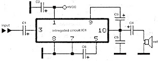
5 8 Watt audio power amplifier

5,8watt amplifier schematics
This amplifier circuit has a power output of a small or too low at 5.8 Watt, which uses IC KA2205. The required voltage for at least 6 volts to 18 volts DC maximum.


Schematics power audio amplifier with IC KA2205

low power amplifier
Component List
C1 = 1uF
C2 = 100uF
C3 = 47uF
C4 = 1000uF
C5 = 0.1uF
C6 = 220uF
IC1 = KA2205

Continue reading...

Wednesday, April 10, 2013

Linear RF Power Meter Circuit

The National Semiconductor LMV225 is a linear RF power meter IC in an SMD package. It can be used over the frequency range of 450 MHz to 2000 MHz and requires only four external components. The input coupling capacitor isolates the DC voltage of the IC from the input signal. The 10-k? resistor enables or disables the IC according to the DC voltage present at the input pin. If it is higher than 1.8 V, the detector is enabled and draws a current of around 5–8 mA. If the voltage on pin A1 is less than 0.8 V, the IC enters the shutdown mode and draws a current of only a few microampères. The LMV225 can be switched between the active and shutdown states using a logic-level signal if the signal is connected to the signal via the 10-kR resistor.
Circuit diagram:
linear-rf-power-meter-circuit-diagram1 Linear RF Power Meter Circuit Diagram
 
The supply voltage, which can lie between +2.7 V und +5.5 V, is filtered by a 100nF capacitor that diverts residual RF signals to ground. Finally, there is an output capacitor that forms a low-pass filter in combination with the internal circuitry of the LMV225. If this capacitor has a value of 1 nF, the corner frequency of this low-pass filter is approximately 8 kHz. The corner frequency can be calculated using the formula fc = 1 ÷ (2 p COUT Ro) where Ro is the internal output impedance (19.8 k?). The output low-pass filter determines which AM modulation components are passed by the detector.

rf-power-meter-circuit-diagram2 
The output, which has a relatively high impedance, provides an output voltage that is proportional to the signal power, with a slope of 40 mV/dB. The output is 2.0 V at 9 dBm and 0.4 V at –40 dBm. A level of 0 dBm corresponds to a power of 1 mW in 50 R. For a sinusoidal wave-form, this is equivalent to an effective voltage of 224 mV. For modulated signals, the relationship between power and voltage is generally different. The table shows several examples of power levels and voltages for sinusoidal signals. The input impedance of the LMV225 detector is around 50 R to provide a good match to the characteristic impedance commonly used in RF circuits.

The data sheet for the LMV225 shows how the 40-dB measurement range can be shifted to a higher power level using a series input resistor. The LMV225 was originally designed for use in mobile telephones, so it comes in a tiny SMD package with dimensions of only around 1 × 1 mm with four solder bumps (similar to a ball-grid array package). The connections are labelled A1, A2, B1 and B1, like the elements of a matrix. The corner next to A1 is bevelled.


http://streampowers.blogspot.com/2012/06/linear-rf-power-meter-circuit.html 
Continue reading...

Sunday, April 7, 2013

Automatic Room Power Control

An ordinary automatic room power control circuit has only one light sensor. So when a person enters the room it gets one pulse and the lights come ‘on.’ When the person goes out it gets another pulse and the lights go ‘off.’ But what happens when two persons enter the room, one after the other? It gets two pulses and the lights remain in ‘off’ state. The circuit described here overcomes the above-mentioned problem. It has a small memory which enables it to automatically switch ‘on’ and switch ‘off’ the lights in a desired fashion. The circuit uses two LDRs which are placed one after another (separated by a distance of say half a meter) so that they may separately sense a person going into the room or coming out of the room.

Outputs of the two LDR sensors, after processing, are used in conjunction with a bicolour LED in such a fashion that when a person gets into the room it emits green light and when a person goes out of the room it emits red light, and vice versa. These outputs are simultaneously applied to two counters. One of the counters will count as +1, +2, +3 etc when persons are coming into the room and the other will count as -1, -2, -3 etc when persons are going out of the room. These counters make use of Johnson decade counter CD4017 ICs. The next stage comprises two logic ICs which can combine the outputs of the two counters and determine if there is any person still left in the room or not. Since in the circuit LDRs have been used, care should be taken to protect them from ambient light.

If desired, one may use readily available IR sensor modules to replace the LDRs. The sensors are installed in such a way that when a person enters or leaves the room, he intercepts the light falling on them sequentially—one after the other. When a person enters the room, first he would obstruct the light falling on LDR1, followed by that falling on LDR2. When a person leaves the room it will be the other way round. In the normal case light keeps falling on both the LDRs, and as such their resistance is low (about 5 kilo-ohms). As a result, pin 2 of both timers (IC1 and IC2), which have been configured as monostable flip-flops, are held near the supply voltage (+9V). When the light falling on the LDRs is obstructed, their resistance becomes very high and pin 2 voltages drop to near ground potential, thereby triggering the flip-flops.

Automatic Room Power Control Circuit DiagramCapacitors across pin 2 and ground have been added to avoid false triggering due to electrical noise. When a person enters the room, LDR1 is triggered first and it results in triggering of monostable IC1. The short output pulse immediately charges up capacitor C5, forward biasing transistor pair T1-T2. But at this instant the collectors of transistors T1 and T2 are in high impedance state as IC2 pin 3 is at low potential and diode D4 is not conducting. But when the same person passes LDR2, IC2 monostable flip-flop is triggered. Its pin 3 goes high and this potential is coupled to transistor pair T1-T2 via diode D4. As a result transistor pair T1-T2 conducts because capacitor C5 retains the charge for some time as its discharge time is controlled by resistor R5 (and R7 to an extent).

Thus green LED portion of bi-color LED is lit momentarily. The same output is also coupled to IC3 for which it acts as a clock. With entry of each person IC3 output (high state) keeps advancing. At this stage transistor pair T3-T4 cannot conduct because output pin 3 of IC1 is no longer positive as its output pulse duration is quite short and hence transistor collectors are in high impedance state. When persons leave the room, LDR2 is triggered first, followed by LDR1. Since the bottom half portion of circuit is identical to top half, this time, with the departure of each person, red portion of bi-color LED is lit momentarily and output of IC4 advances in the same fashion as in case of IC3. The outputs of IC3 and those of IC4 (after inversion by inverter gates N1 through N4) are ANDed by AND gates (A1 through A4) and then wire ORed (using diodes D5 through D8).

The net effect is that when persons are entering, the output of at least one of the AND gates is high, causing transistor T5 to conduct and energize relay RL1. The bulb connected to the supply via N/O contact o relay RL1 also lights up. When persons are leaving the room, and till all the persons who entered the room have left, the wired OR output continues to remain high, i.e. the bulb continues to remains ‘on,’ until all persons who entered the room have left. The maximum number of persons that this circuit can handle is limited to four since on receipt of fifth clock pulse the counters are reset. The capacity of the circuit can be easily extended to handle up to nine persons by removing the connection of pin 1 from reset pin (15 and utilizing Q1 to Q9 outputs of CD4017 counters. Additional inverters, AND gates and diodes will, however, be required.
Continue reading...

Saturday, April 6, 2013

New architecture silicon microwave power transistor

high power transistor

Above is a new architecture of the transistor which is applied in high voltage vertical FET (HVVFET ™) to achieve high operating voltage and very high power packaging density. This approach offers many advantages to designers of power amplifiers.
High voltage solutions help designers to simplify the matching circuit discrete devices. Achieving high power through the device causing high voltage impedance level, allows the network to the appropriate circuit with fewer components smaller area. As a result, a series of matching not only the smaller, less expensive solutions, but offers higher reliability as well as there fewer parts with the potential to fail. This circuit is suitable also show less loss than a low impedance solution that has a higher transformation 50 ohm impedance ratio desired.
Continue reading...

Friday, April 5, 2013

Simple 240VAC TO 5VDC POWER SUPPLY

This is simple way to power some 5v logic from a 240vac source. If a 120vac power adapter is used, the circuit will also work for 120vac power lines.
 
 
240VAC TO 5VDC POWER SUPPLY,
Continue reading...

Thursday, April 4, 2013

Reducing L200 Power Dissipation Circuit using Series Resistor


It’s good to reduce the power dissipated by the device. Using resistor connected in series to the input (the left figure) is a simple and economic method to reduce the device input-output differential voltage. This is the figure of the design circuit;


Here’s the formula for calculating R:
R= [Vi min- (Vo+Vdrop)]/Io
Vdrop = minimum differential voltage between the input and the output of the device at current Io
Vin min = minimum voltage
Vo = Output voltage
Io = output current

Resistor R can be connected between pins 1 and 2 of the IC instead of in series with the input if the load is constant (the right figure). So, part of the load current flows through the device and part through the resistor. This configuration is available when the minimum current by the load is:
Io min = Vdrop/R


Continue reading...

Tuesday, April 2, 2013

Fuse Box BMW 325i 1992 Convertible Power Distribution Diagram

Fuse Box BMW 325i 1992 Convertible Power Distribution Diagram - Here are new post for Fuse Box BMW 325i 1992 Convertible Power Distribution Diagram.

Fuse Box BMW 325i 1992 Convertible Power Distribution Diagram


Fuse Box BMW 325i 1992 Convertible Power Distribution Diagram

Fuse Panel Layout Diagram Parts: Service Interval Indicator, Tachometer/Fuel Economy Gauges, Gauges/Indicators;, Brake Warning System, Back Up Lights, On Board Computer, Start, Injection Electronics, Active Check Contro, Cruise Control, Injection Electronics, Radio/Antenna, Speedometer/Indicators, On Board Compute, Front Park/Tail, Horn, Rear Defogge, Injection Electronics, Ignition Key Warning/Seatbelt Warning, Auxiliary Fan, Auto Chraging Flashlight, Ignition Key Warning/Seatbelt WarninActive Check Control, Lights, Interior Lights , Central Locking, Radio/Antenna, On Board Computer, Cigar Lighter, Radio/Antenna, Heated/Air Conditioning, Active Check Control, Front Side Marker, Headlights, High Beam Indicator, Headlight, Auxiliary Fan, Lights, Turn/Hazard Warning, Wiper/Washer, Stop Lights, Active Check Control, Antilock Braking System;, Cruise Control, Map Reading Light, Headlights, Heated Seats, Power Windows, Auxiliary Fan, Auxiliary Fan, Interior Light, Power Mirrors, Injection Electronics, Interior Lights, Radio/Antenna, Trunk Light, Active Check Control, Service Interval Indicator, On Board Computer, Tachometer/Fuel Economy Gauge, Electro Mechanical Convertible Top.
Continue reading...

Thursday, March 28, 2013

Transformerless Power Supply

This circuit will supply up to about 20ma at 12 volts. It uses capacitive reactance instead of resistance; and it doesnt generate very much heat.The circuit draws about 30ma AC. Always use a fuse and/or a fusible resistor to be on the safe side. The values given are only a guide. There should be more than enough power available for timers, light operated switches, temperature controllers etc, provided that you use an optical isolator as your circuits output device. (E.g. MOC 3010/3020) If a relay is unavoidable, use one with a mains voltage coil and switch the coil using the optical isolator.C1 should be of the suppressor type; made to be connected directly across the incoming Mains Supply.

They are generally covered with the logos of several different Safety Standards Authorities. If you need more current, use a larger value capacitor; or put two in parallel; but be careful of what you are doing to the Watts. The low voltage AC is supplied by ZD1 and ZD2. The bridge rectifier can be any of the small Round, In-line, or DIL types; or you could use four separate diodes. If you want to, you can replace R2 and ZD3 with a 78 Series regulator. The full sized ones will work; but if space is tight, there are some small 100ma versions available in TO 92 type cases. They look like a BC 547. It is also worth noting that many small circuits will work with an unregulated supply.

Transformerless Power Supply Circuit Diagram
You can, of course, alter any or all of the Zenner diodes in order to produce a different output voltage. As for the mains voltage, the suggestion regarding the 110v version is just that, a suggestion. I havent built it, so be prepared to experiment a little. I get a lot of emails asking if this power supply can be modified to provide currents of anything up to 50 amps. It cannot. The circuit was designed to provide a cheap compact power supply for Cmos logic circuits that require only a few milliamps. The logic circuits were then used to control mains equipment (fans, lights, heaters etc.) through an optically isolated triac.

If more than 20mA is required it is possible to increase C1 to 0.68uF or 1uF and thus obtain a current of up to about 40mA. But suppressor type capacitors are relatively big and more expensive than regular capacitors; and increasing the current means that higher wattage resistors and zener diodes are required. If you try to produce more than about 40mA the circuit will no longer be cheap and compact, and it simply makes more sense to use a transformer. The Transformerless Power Supply Support Material provides a complete circuit description including all the calculations.

Web-masters Note:

I have had several requests for a power supply project without using a power supply. This can save the expense of buying a transformer, but presents potentially lethal voltages at the output terminals. Under no circumstances should a beginner attempt to build such a project.

Important Notice:

Electric Shock Hazard. In the UK,the neutral wire is connected to earth at the power station. If you touch the "Live" wire, then depending on how well earthed you are, you form a conductive path between Live and Neutral. DO NOT TOUCH the output of this power supply. Whilst the output of this circuit sits innocently at 12V with respect to (wrt) the other terminal, it is also 12V above earth potential. Should a component fail then either terminal will become a potential shock hazard.

MAINS ELECTRICITY IS VERY DANGEROUS.

If you are not experienced in dealing with it, then leave this project alone. Although Mains equipment can itself consume a lot of current, the circuits we build to control it, usually only require a few milliamps. Yet the low voltage power supply is frequently the largest part of the construction and a size-able portion of the cost.
Continue reading...

Wednesday, March 27, 2013

Alternative Halogen Power Supply

Readers who do not care to modify the power supply of an old PC into a suitable halogen power source (see our April 2006 issue), may find the present design a welcome alternative. The circuit does not need any changes to the power supply. It allows the halogen lamps to be initially powered from the 5V rail of the supply via RE2, so that they are preheated. Subsequently, they are powered from the 12-V rail via RE1, while at the same time the 5-V rail is disconnected.

This ensures that the current surge through the lamps is so small that the protection in the power supply does not react. Operation of the circuit is as follows. As soon as the PC supply provides power, IC1.B drives T1 into conduction and RE2 closes. The potential at the non-inverting input of IC1.B is 6 V, while that at the inverting input rises from 0 V. Lamp LA1 is then connected to the 5-V rail.

Circuit diagram:
alternative halogen power supply circuit schematic
Alternative Halogen Power Supply Circuit Diagram

After a short span of time, the voltage across C1 has risen to a value where IC1.B changes over, whereupon T1 is cut off. At the same time, IC1.A drives T2 into conduction. The circuit is then decoupled from the 5-V rail and connected to the 12-V terminal. The 5-V rail in the PC power supply is protected against spikes on the 12-V line by D1. Diode D2 protects IC1 against over-voltage on its inputs should the 12-V rail fail.

Resistors R4 and R5 limit the base currents of the transistors. D3 and D4 are quenching diodes. The time during which lamp LA1 is powered by 5 V is preset with potentiometer P1. The maximum time span is about 0.33 s and the minimum 3.3 ms. The latter is perhaps rather short, but it also depends to some extent on the type of power supply used. Some experimentation may be worthwhile!
Author: Stijn Coenen - Copyright: Elektor Electronics
Continue reading...

Monday, March 25, 2013

Fuse Box Ford 1998 Exposition Power Distribution Diagram

Fuse Box Ford 1998 Exposition Power Distribution Diagram - Here are new post for Fuse Box Ford 1998 Exposition Power Distribution Diagram.

Fuse Box Ford 1998 Exposition Power Distribution Diagram


Fuse Box Ford 1998 Exposition Power Distribution Diagram

Fuse Panel Layout Diagram Parts: fuse panel, blower motor relay, 4 wheel anti lock brake system, power monroof, ignition switch, starter relay, transfer case relay, automatic relay control, adaptive suspension, compressor, PCM power relay, rear window control, fog lamp, daytime running lamp, air bag diagnostic, powertrain control module, rear wiper, fuel pump, park lamp relay, dimmer relay, headlamp relay, illumination, headlamp, heated oxygen sensor, camshaft, automatic transmission, voltage regulator, electronic engine control.
Continue reading...

Friday, March 22, 2013

LM390 power amplifier schematic

Circuit schematic above is / include power amplifiers that have low power output. 1 Watt output power is only based on the IC , and ic used LM390 , manufactered by NS and ic packaged in DIP-14. For output impedance have 4 OHm. Requires a minimum voltage 4 Volt and Maximum voltage is only 9Volt.
Part List :

Resistor
R1________33K
R2________510R
R3________510R
R4________2.7R

Capacitor
C1________100uF 16V
C2________100uF 16V
C3________10uF   16V
C4________220uF 35V
C5________10uF   16V
C6________100n

IC
IC1_______LM390 
Continue reading...

Thursday, March 21, 2013

Switch Mode Power Supply

National Semiconductor has been producing and designing ICs for use in switch-mode power supplies for many years. The application of these devices is normally straightforward, helped by the excellent documentation that is available. A typical example of a switch-mode power supply is that based on the LM2671 or LM2674. The components for it are available for outputs of 3.3 V, 5 V and 12 V. There is also a version providing a presettable output voltage. Within the specified application, the supplies can deliver currents of up to 500 mA. Note-worthy is the high switching frequency of 260 kHz.

Switch-mode power supply circuit diagramThis has the advantage that only low-value inductor and capacitors are needed, and this results in excellent efficiency and small dimensions. In normal circumstances, the efficiency is 90% and may even go up to 96%. Both ICs provide protection against current and temperature overloads. The LM2671 has a number of additional facilities such as soft start and the option to work with an external clock. The latter enables several supplies to be synchronized so as to give better control of any EMC (ElectroMagnetic Compatibility). The application shown in the diagram provides an output voltage of 5 V and an output current of up to 500 mA. Diode D1 is a Schottky type (Uco≥ 45 V and Imax≥ 3 A).
Continue reading...

Wednesday, March 20, 2013

6610 7210 can not power on

Nokia 6610, nokia 7210 can not power on after flashing done.
Check this circuit, jumper if needed,


Continue reading...